Table Of Content

Laying out traces for routing and copper placement, or managing the layer needed for solder can become difficult without an accurate and reliable integration from schematic capture to layout. Between the copper foil/copper sheeting and the core layer, there may be a layer of pre-impregnated resin, or prepreg. It is then sandwiched between the core and the layer of copper foil, or between layers of copper foil. During the bonding process, heat and pressure are applied, sandwiching the prepreg down and activating the epoxy so it bonds the core and the copper or the copper and the copper together. Thermal management is another critical aspect of component placement. Heat-generating components, such as power regulators or high-speed processors, should be placed in a way that allows for efficient heat dissipation.
Eagle Software Download. Autodesk EAGLE is a PCB (Printed… by plchmiservo - Medium
Eagle Software Download. Autodesk EAGLE is a PCB (Printed… by plchmiservo.
Posted: Sat, 03 Feb 2024 08:00:00 GMT [source]
How Are PCBs Manufactured?
After checking your layout against your design rules, you can generate manufacturing output documentation for your fabricator. This includes Gerber files, pick-and-place files, assembly drawings, and much more. Altium makes panelization easy, including the ability to evaluate 3-D views to determine the best panel arrangement. It’s easy enough to create schematic symbols and PCB footprints with Altium Designer, but everyone needs resources to stay inspired and overcome design challenges.
PCB Manufacturing Challenges and Considerations
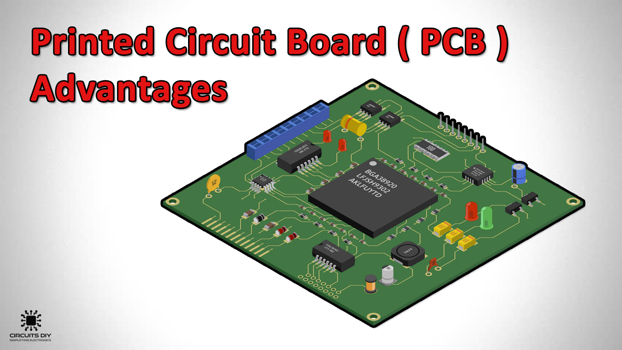
Vias are an important part of PCB design, as they allow for complex circuits to be created with multiple layers and connections. They are used in a wide range of applications, from simple electronic devices to complex computer systems. Attached to the copper traces — the pads and paths — of the printed circuit board are the components. These are the things that give the printed circuit board its purpose and are usually installed solely with that purpose in mind. If the substrate board is the skeleton and the copper traces are the musculature, then the components are the vital organs — they are what allow the PCB to function in its intended purpose.
Local PCB Layout Tweaks for Improved Signal Integrity When Using ESD Protection Devices - In Compliance
Local PCB Layout Tweaks for Improved Signal Integrity When Using ESD Protection Devices.
Posted: Sun, 01 Oct 2023 07:00:00 GMT [source]
Section 15 – PCB Design: Creating a Document Package
These steps help optimize the design for efficient production and assembly. Creating a PCB involves tasks such as creating the schematic, simulating the circuitry, setting up the CAD tool, placing components, and routing the PCB. Once the design is finalized, PCB manufacturing and assembly take place. This involves the fabrication of the PCB and the placement of components onto the board. Remember, the world of PCB design is constantly evolving, and it's important to stay updated with the latest advancements and best practices. With NextPCB, you can create high-quality PCBs that meet your project's requirements.
If you’re new to the printed circuit design world, most modern PCB board design concepts will start with a 4-layer board on FR4, although you can define any number of layers you like in Altium Designer. You can also take advantage of the Materials Stackup Library; this lets you choose from a range of different laminates and unique materials for your printed circuit board. After you’ve created your schematic, for the next PCB design step you’ll need to use the schematic capture tool in Altium Designer to import components into a blank PCB layout.
Simulation-Driven Design in Your Schematic

It is a good idea to include reference designators for components as this will assist in PCB board assembly. Also, make sure to keep any polarity indicators, pin 1 indicators, and any other labels visible as these will aid PCB assembly and testing. You can also add a company logo and part numbers using the image tools and text tools in the PCB Editor. These elements need to be placed in the Top Overlay or Bottom Overlay layers in the PCB layout. Altium Designer includes a number of important tools to help make your routing experience easier and more productive. There is an autorouter engine that uses a modern algorithm to route traces, as well as traverse layer pairs with vias.
The first step is to develop the library CAD parts needed for the design. This will include schematic symbols, simulation models, footprints for PCB layout, and step models for 3D printed circuit board display. Once the libraries are ready, the next step is to create the logical representation of the circuitry on a schematic. CAD tools are used to place the symbols on a schematic sheet and then connect them to form the circuitry.
The rigid sections, made from standard FR-4 material, provide structural support and accommodate components that require stability. The flexible sections, made from thin, flexible materials such as polyimide, allow for bending and folding in specific areas and are typically used to connect the rigid sections, creating a three-dimensional PCB assembly. Multi-layer PCBs consist of three or more conductive layers, separated by prepreg (pre-impregnated) insulating layers. The conductive layers are typically made of copper foil, and the insulating layers are bonded together using heat and pressure in a lamination process. The inner layers of a multi-layer PCB can be used for power and ground planes, while the outer layers are used for signal routing and component placement. The cost of a custom printed circuit board (PCB) can vary widely depending on a variety of factors, including the size, complexity, number of layers, and the quantity needed.
Source Data Extended Data Fig. 8
Electronic components are then attached to this board using a metal to conduct electricity. The metal etched into the board allows electricity to travel from one component to another in electrical circuits. The "card" is made of a material that does not conduct electricity, usually fiberglass. Usually copper is etched (set in thin lines) inside the board between the layers of fiberglass, or on the surface of the board.
The team’s process to create the vPCB deviated only slightly from those used for PCBs. Conventionally, semi-cured PCB layers are held in cool, dry conditions where they have a limited shelf life before they’re laminated in a heat press. Because vitrimers can form new bonds, researchers laminated fully cured vPCB layers. The researchers found that to recycle the vPCBs they could immerse the material in an organic solvent that has a relatively low boiling point.
All authors contributed to the study concept and experimental methods, discussed the results and edited the manuscript. The manufacturer is even working on a vertical lift system that could change how aircraft take off. The Winona, MN, division of Benchmark Electronics, Inc. has 650 employees.


No comments:
Post a Comment